Thermal evaporation technique thin film deposition pdf
Disadvantages of Sputter Deposition • Sputtering rates are low compared to those that can be attained in thermal evaporation. • Sputtering targets are often expensive.
Understanding Thin Film Process Technologies Learn about the different coating process technologies and where each is best employed. There are currently a number of different processes used for the manufacture of optical thin films, the most common of these being traditional thermal or electron beam evaporation, ion assisted deposition (IAD) and ion beam sputtering (IBS).
thin film deposition techniques – steps towards more sustainable packages Mika Vähä‐Nissi 1 , Terhi Hirvikorpi 1 , Tuomas Mustonen 1 , Maarit Karppinen 2 , Ali Harlin 1 1 VTT Technical Research Centre of Finland, Espoo, Finland
PVD Recipes ROCHESTER INSTITUTE OF TECHNOLOGY MICROELECTRONIC ENGINEERING Physical Vapor Deposition – Evaporation and Sputtering Dr. Lynn Fuller
Among physical vapor deposition techniques thermal evaporation (TE) is the one with the longest standing tradition. However, during the last 30 years of booming semiconductor industry which involves a great deal of thin film technology, deposition techniques like CVD (chemical vapor deposition) or sputtering which often offer unquestionable advantages have been developed to perfection and TE
5 Thin Film Deposition Techniques 5.1. Introduction As already pointed out in Chapter 1, a deposition technique and its associated process parameters have a characteristic effect on the
Evaporation is a common method of thin-film deposition. The source material is evaporated in a vacuum. The vacuum allows vapor The source material is evaporated in …
Thin films of Ge33As12Se55 were produced using two deposition techniques, ultra-fast pulsed laser deposition (UFPLD) and thermal evaporation (TE), and their properties have been investigated. The chemical composition of the UFPLD films was virtually identical to the composition of the chalcogenide glass targets, whereas the composition of films deposited by TE was significantly different from
Evaporation is a common method of thin-film deposition. The source material is evaporated in a vacuum. The vacuum allows vapor particles to travel directly to the target object (substrate), where they condense back to a solid state.
CdTe thin films were deposited by thermal evaporation technique at different power. Thermally evaporated CdTe thin films were then subjected to post deposition laser annealing. The effect of laser
Mylar films were deposited on ultrasonically cleaned optically flat glass slides and subjected to a ‘‘scotch tape’’ adhesion test.
Thin film deposition University of Colorado Boulder

Signature of growth-deposition technique on the properties
Thermal Evaporation. When a pan of water is left to boil on the stove, droplets of water form on the ceiling of the kitchen. If the boiling water is then transfered to a bowl and quickly placed in the freezer, a layer of ice forms above the bowl.
The Deposition of Bi 2 Te 3 and Sb 2 Te 3 Thermoelectric Thin-films by Thermal Co-Evaporation and Applications in Energy Harvesting L.M. Goncalves University of Minho, Dept. of Industrial Electronics, Azurem, 4800-058 Guimaraes, Portugal
of the thin film deposition technique as given on next page. The vacuum evaporation technique which is lies in PVD employed by us can be subdivided in to following parts: (1) Thermal Evaporation (2) Electron Beam (3) Laser Beam In the present work we have used vacuum thermal evaporation technique to prepare the samples. 2.2 VACUUM THERMAL EVAPORATION: 2.2.1: Kinetics The vacuum thermal
Broadly, the important methods of thin film deposition are classified as physical deposition and chemical deposition. Physical deposition method is again classified into thermal evaporation, electron beam evaporation, molecular beam
In general, thin film is a small thickness that produces by physical vapour deposition (PVD) and chemical vapour deposition (CVD). Despite the PVD technique has a few… Despite the PVD technique
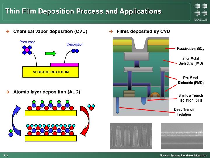
Chemical vapor deposition (CVD) forms a thin film on the surface of a substrate by thermal decomposition and/or reaction of precursor molecules (gaseous compounds) Silicon : SiH

Physical Vapor Deposition: Evaporation and Sputtering Reading: Chapter 12. Georgia Tech ECE 6450 – Dr. Alan Doolittle Evaporation Evaporation and Sputtering (Metalization) For all devices, there is a need to go from semiconductor to metal. Thus we need a means to deposit metals. Many of these techniques used for metal deposition can be used to deposit other materials as well. Several …
29/04/2014 · Physical vapor deposition by resistant evaporation technique. E:Mail:info@thinfilmscience.com.
The most significant process for optical coating is the variant of vacuum deposition. Zinc sulfide having direct and large band gap which is use in optoelectronics. By using ZnS material in thermal evaporation technique and characterizing the minimum reflectance and maximum transmittance in visible wavelength and energy gap increases with
Thermal evaporation of metals having low to moderate deposition rates (10–100 nm/min) is regarded as one of the traditional physical vapor deposition (PVD) techniques. It relies on the sublimation of material onto a substrate in a vacuum. In industrial applications, …
1 Signature of growth-deposition technique on the properties of PECVD and thermal SiO 2 Subimal Majee 1*, Devesh Barshilia , Sanjeev Kumar , Prabhash Mishra2 and
Fabrication of Microsystems Wafer Cleaning Deposition (Evaporation, sputtering, CVD, etc) [Metals, Semiconductors, Dielectrics] Resist processing & Pattern
Typically, thin (<100nm) film molecular organic electronic devices such as organic light emitting devices (OLEDs), are grown by vacuum thermal evaporation (VTE), permitting the high degree of purity, pattern, and structural control needed for high
The vacuum thermal evaporation deposition technique consists in heating until evaporation of the material to be deposited. The material vapor finally condenses to form of thin film on the cold substrate surface and on the vacuum
thermal evaporation is more suitable because of its ability to deposit multiple films, friendly environment, non-pollutant, thermal temperature, easy to control the growth factors like film thickness and deposition rate [5].
Thin Film Deposition can be achieved through two methods: Physical Vapour Deposition (PVD) or Chemical Vapour Deposition (CVD) Physical Vapor Deposition (PVD) comprises a group of surface coating technologies used for decorative coating, tool coating, and other equipment coating applications. It is fundamentally a vaporization coating process in which the basic mechanism is an atom by atom

Thin Film Deposition Processes Dler Adil Jameel1, 2, * 1School of Physics and Astronomy, it can be seen that the thermal evaporation technique is more favourable than sputtering technique for depositing thin film for many materials that low and high melting materials, especially, metals. 2.3. Advantages and Disadvantages of PVD Process Nothing is ever perfect; everything has negative and
Thin Film Deposition 6 Advantages and Disadvantages over Thermal Evaporation Advantages! Low contamination of the deposited thin films .! Improved control of deposition rate.
Thermal evaporation is a popular physical vapor deposition technique because of its simplicity. During this process, a material in a high-vacuum environment is heated to its evaporation point by joule heating of the resistive boat in which it is located.
Thin film deposition is a process whereby materials – generally precious metals or oxides – are deposited onto a substrate or lithography sample. This can be achieved in a variety of ways such as sputtering, electroplating, evaporation, or CVD. MCN offers a range of different thin film deposition techniques and instruments, which are briefly explained here. Process: Make & Model Defining
vacuum thermal evaporation Vacuum evaporation is also known as vacuum deposition and this is the process where the material used for coating is thermally vaporized and then proceeds by potential differences to the substrate with little or no collisions with gas molecules.
THIN FILM DEPOSITION FORMATION OF NANOPARTICLES
Sputter deposition is widely used to deposit thin film metallization on semiconductor material, coatings on architectural glass, reflective coating on polymers, magnetic films for storage media,
Thin film deposition was once considered a black art. Evaporation, sputter deposition and chemical vapour deposi- tion were routinely used, but there was very little under-
In this present study, Copper thin film deposition on steel substrates by thermal evaporation method at room temperatureis prepared. The sequential structure and morphology of copper
THIN FILM & NANOTECHNOLOGY Thermal Evaporation System . Vacuum evaporation is one of the most cost-effective deposition techniques. It’s also one of the oldest techniques, considering that Thomas Edison himself stated “the uses of this invention are unlimited.” Edison was not correct, however, as thermal evaporation has a number of limitations including evaporation temperature – guy hires film crew to document his murders Thermal Evaporation Sources Technical Notes We examine methods of manufacturing thin film and deposition sources in Vacuum Systems. Deposition sources are components that, through a variety of techniques, facilitate a physical or chemical change in a base material in order to make it useful for creating thin films.
Other techniques for deposition of compounds include thermal evaporation of the compound (as is performed for salt coatings), sputtering of the compound, and reactive sputtering or evaporation.
substrate by thermal evaporation and pulsed laser deposition (PLD) methods. CuPc thin films CuPc thin films prepared at different annealing temperatures (298, 323, 348, 373, 423K) respectively.
Keywords: Chalcogenide glasses; thermal evaporation; thin film; laser irradiation effect; thin films by using thermally evaporated deposition technique and to investigate the influence of laser-irradiation and effect of thickness on their optical properties. II. Experimental Details In 6 Se 7 compound was synthesized first, by mixing and melting the high purity (99.999%) individual
In this work, the authors compare the morphological, structural, nanomechanical, and microtribological properties of Pb films deposited by thermal evaporation (TE) and pulsed laser deposition (PLD) techniques onto Si (111) substrates.
2 • Physical Vapor Deposition (PVD) – Film is formed by atoms directly transported from source to the substrate. • Evaporation • Sputtering • Chemical Vapor Deposition (CVD)
When used to apply very thin films in a high vacuum environment, this process is known as ‘thermal evaporation’. The heat is provided either by Joule heating via a refractory metal element (resistive evaporation), or directly from a focussed beam of high energy electrons (electron beam evaporation). Other deposition techniques, such as laser ablation or a cathodic arc deposition, use
E-Beam evaporation is a physical vapor deposition (PVD) technique whereby an intense, electron beam is generated from a filament and steered via electric and magnetic fields to strike source material (e.g. pellets of Au) and vaporize it within a vacuum environment.
Sains Malaysiana 43(7)(2014): 1061–1067 Deposition and Characterization of SnSe and CuInSe 2 Thin Films by Thermal Evaporation Technique from Synthesized SnSe and CuInSe
In this chapter, we discuss some advance techniques and principles of thin-film depositions. The vacuum thermal evaporation technique, electron beam evaporation, pulsed-layer deposition, direct current/radio frequency magnetron sputtering, and chemical route deposition systems will be discussed in detail. Thin films have a great impact on the modern era of technology. Thin films are considered
technique has been the most suitable method owing to high Keywords— CdTe thin film, thermal evaporation, thermal deposition rate, low material consumption and low cost of annealing, solar cell. operation [24]. The purpose of this paper is to analyse the I. INTRODUCTION effect of thermal annealing on the structural and optical properties of CdTe thin films grown by thermal evaporation
The E-Beam, Thermal Evaporation & Ion Assisted System is completely customizable; Vacuum evaporation is one of the most cost-effective deposition techniques.
23-1 Thin Films: An Introduction Deposition of thin films has been of interest for almost 100 years examples solar panels oxide thin film on a substrate
Physical Vapor Deposition – Evaporation and Sputtering Dr
graded film composition along the film thickness. Vacuum Evaporation Sources • Physical evaporation – A “source” container is heated. – The material to be evaporated is placed in or near the source. – The radiative and conductive heating evaporates the source. • Electron beam evaporation – A filament is heated and emits electrons. – The electrons heat the evaporant and
Thin film deposition systems & equipment. RF & DC Sputtering, E-Beam evaporation, low temperature Organic sources & Thermal evaporation. Glovebox compatible.
96 Thin-Film Evaporation Processes the late 1960s evaporation surpassed sputtering as the preferred film deposition technique. Higher deposition rates, better vacuum and cleaner
Among these methods, the thermal evaporation technique is the most interesting technique because the advantages of this technique have high stability, high reproducibility, high deposition rate, large area deposition, and non-expansive. This technique provides economical and efficient use of evaporate material enabling constant rate of deposition. The aim of the present study is to …
AJA International ATC-M Series Multi-Technique Systems are versatile tools that combine various thin film deposition, ion milling and analytical operations in a single chamber (Hybrid Systems) or in multiple chambers (Multi-Chamber Systems) to allow the in-situ transfer of substrates from process to process without breaking vacuum.
Multi-Technique Thin Film Deposition / Analysis Systems

CHAPTER 2 THIN FILM PREPARATION METHODS
Thin Film Deposition Physical Vapor Deposition (PVD) – Film is formed by atoms directly transported from source to the substrate through gas phase • Evaporation • Thermal evaporation « • E-beam evaporation « • Sputtering • DC sputtering « • DC Magnetron sputtering « • RF sputtering « • Reactive PVD Chemical Vapor Deposition (CVD) – Film is formed by chemical reaction on
Thin Film Deposition Techniques & Capabilities Thermal Evaporation Sources. Thermal Evaporation. Thermal evaporation sources include components that evaporate the base material through the use of resistive element heating.
In the present paper, Copper Phthalocyanine (CuPc) thin films were deposited on glass and silicon substrate by thermal evaporation and pulsed laser deposition (PLD) methods.
E-Beam Thermal Evaporation and Ion Assisted System

Deposition and Patterning Techniques for Organic Materials
CHAPTER 2 THIN FILM PREPARATION METHODS 2 either thermal evaporation or an impact process. Thin film deposition by chemical methods, include thin film formation by chemical processes in the gas or vapor phase as well as from liquid phases. The broad classification of thin film deposition techniques [1-6] is outlined in Fig. 2.1. 2.2 CHEMICAL METHODS Unlike the physical …
The most important factor in thermal evaporation technique is the high vacuum, which can minimize the interaction between the residual gases and the sensitive surface of growing films. For preparation of thin films and electrodes a conventional coating unit (Vacuum Coater, Hindhivac 12A4D, and …
Thermal evaporation deposition is the most basic method used to produce thin films. Physical vapor deposition (PVD) is just one method of producing thin films. Michael Faraday pioneered the first PVD process in the early 1800’s [1]. The semiconductor industry relies heavily on thin film technology to produce flash memory and computer chips. thermal. and plasma arc deposition methods. Powell.
Choice of the deposition technique Thickness Uniformity Nanomorphology (molecules relative arrangement in the solid state) solvent evaporation deposition rate
Influence of Thermal Annealing on CdTe Thin Film Deposited
Thin Film Deposition Hivatec Laboratory
Deposition of thin films has been of interest for almost
– CHARACTERIZATION OF ZINC OXIDE (ZnO) THIN FILM COATED
The Deposition of Bi2Te3 and Sb2Te3 Thermoelectric Thin


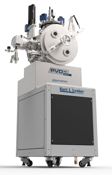
Kurt J. Lesker Company Thermal Evaporation Sources
Lecture 12 Physical Vapor Deposition Evaporation and
Comments
8 responses to “Thermal evaporation technique thin film deposition pdf”
1 Signature of growth-deposition technique on the properties of PECVD and thermal SiO 2 Subimal Majee 1*, Devesh Barshilia , Sanjeev Kumar , Prabhash Mishra2 and
Structural and Surface Morphology Analysis of Copper
In this present study, Copper thin film deposition on steel substrates by thermal evaporation method at room temperatureis prepared. The sequential structure and morphology of copper
ICFM313 Characterization Study of Copper Thin Film Coated
Studies on Optical Properties of ZnS Thin Film by Thermal
Thermal evaporation is a popular physical vapor deposition technique because of its simplicity. During this process, a material in a high-vacuum environment is heated to its evaporation point by joule heating of the resistive boat in which it is located.
Thin Film Deposition Hivatec Laboratory
Effect of substrate temperature on ZnS films prepared by
29/04/2014 · Physical vapor deposition by resistant evaporation technique. E:Mail:info@thinfilmscience.com.
Influence Of Laser Irradiation On The Optical Properties
ICFM313 Characterization Study of Copper Thin Film Coated
Thin Film Evaporation Systems Thermal E-Beam
In this work, the authors compare the morphological, structural, nanomechanical, and microtribological properties of Pb films deposited by thermal evaporation (TE) and pulsed laser deposition (PLD) techniques onto Si (111) substrates.
Thin Film Deposition Processes files.aiscience.org
CHARACTERIZATION OF ZINC OXIDE (ZnO) THIN FILM COATED
Thin Film Deposition Techniques & Capabilities Thermal Evaporation Sources. Thermal Evaporation. Thermal evaporation sources include components that evaporate the base material through the use of resistive element heating.
THIN FILM DEPOSITION FORMATION OF NANOPARTICLES
Thermal evaporation is a popular physical vapor deposition technique because of its simplicity. During this process, a material in a high-vacuum environment is heated to its evaporation point by joule heating of the resistive boat in which it is located.
Effect of substrate temperature on ZnS films prepared by
vacuum thermal evaporation Vacuum evaporation is also known as vacuum deposition and this is the process where the material used for coating is thermally vaporized and then proceeds by potential differences to the substrate with little or no collisions with gas molecules.
Kurt J. Lesker Company Thermal Evaporation Sources